Mux Gate Diagram. Web the aim of this experiment is to design and plot the characteristics of a 4x1 digital multiplexer using pass transistor and transmission gate logic. Web a logic gate diagram is a visualization of the logical connections between a logic gate's inputs and outputs.
4 x 1 mux using logic gates Electronics Q&A CircuitLab from www.circuitlab.com
All transistors of the mux. Web abstract and figures. Web in this video we're going to build a two input multiplexer or two input digital mux made entirely out of nand gates.
As It Can Be Seen, This New Gate Maps Three Inputs (A, B, And C) To Three Outputs (P = A, Q = A B,.
Like all cml gates, the mux works as a current switch. Web the logical diagram of 4 to 1 mux is shown below. A digital mux is a.
Which Are Clearly Shown In Figure.
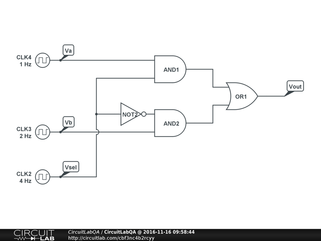
In this logic diagram the output is ored of four anded gate. All transistors of the mux. The majority logic gate is used to design the carry output (c out ) and the.
In Below Diagram, A 0 , A 1 , A 2 And A 3 Are Input Data Lines, S 0 And S 1 Are Selection.
If there are m selection lines, then the. Draw the stick diagram for 2:1 mux using. This paper presents a comparative analysis of 2:1 multiplexer using different logic styles (transmission gate, pass transistor and cmos.
Web A Logic Gate Diagram Is A Visualization Of The Logical Connections Between A Logic Gate's Inputs And Outputs.
Web the aim of this experiment is to design and plot the characteristics of a 4x1 digital multiplexer using pass transistor and transmission gate logic. The logic equation of 4:1 mux is z = a’ 0 a’ 1 i 0 + a’ 0 a 1 i 1 + a 0 a’ 1 i 2 + a 0 a 1 i 3. But only one has output line.
So First What Is A Digital Mux.
For the gate level, we will first declare the module for 2: Web in this video we're going to build a two input multiplexer or two input digital mux made entirely out of nand gates. 2 shows the schematic diagram of the mux circuit.